- 您现在的位置:买卖IC网 > Sheet目录3882 > PIC24F08KL301-I/SS (Microchip Technology)IC MCU 16BIT 8KB FLASH 20-SSOP
CHAPTER 8 8-BIT TIMER/EVENT COUNTERS 2 TO 5
User’s Manual U15905EJ2V1UD
242
8.3
Control Registers
The following two registers are used to control 8-bit timer/event counter n.
Timer clock selection register n (TCLn)
8-bit timer mode control register n (TMCn)
Remark
To use the functions of the TIn and TOn pins, refer to Table 4-18 Using Alternate Function of Port
Pins.
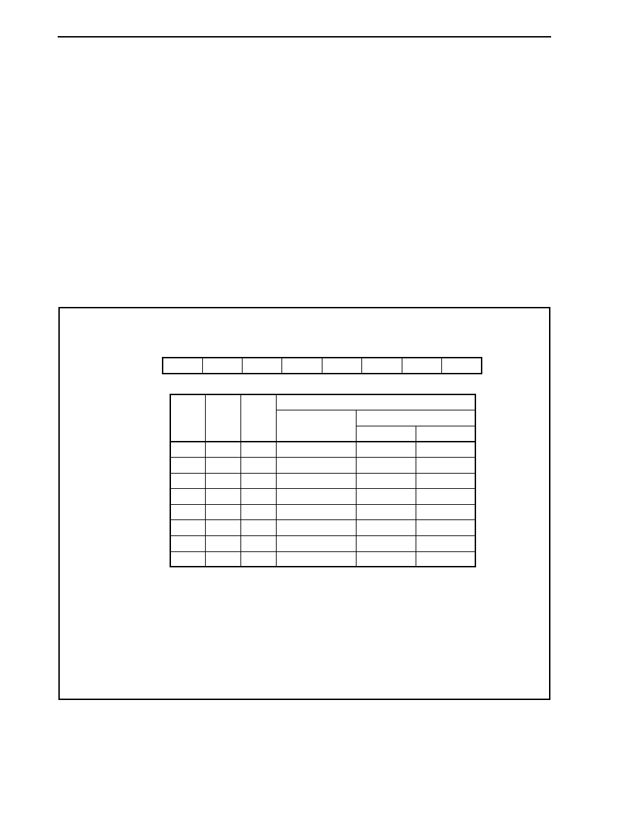
(1) Timer clock selection registers 2 to 5 (TCL2 to TCL5)
These registers set the count clock of 8-bit timer/event counter n and the valid edge of the TIn pin input.
The TCLn register can be read or written in 8-bit units.
These registers are cleared to 00H after reset.
(a) Timer clock selection registers 2 and 3 (TCL2 and TCL3)
Falling edge of TIn
Rising edge of TIn
fXX/4
fXX/8
fXX/16
fXX/32
fXX/128
fXX/512
Count clock selection
TCLn2
0
1
TCLn1
0
1
0
1
TCLn0
0
1
0
1
0
1
0
1
20 MHz
10 MHz
200 ns
400 ns
800 ns
1.6
s
6.4
s
25.6
s
400 ns
800 ns
1.6
s
3.2
s
12.8
s
51.2
s
Clock
fXX
0
TCLn
(n = 2, 3)
0
TCLn2
TCLn1
TCLn0
After reset: 00H
R/W
Address: TCL2 FFFFF644H, TCL3 FFFFF645H
7
6
54
32
1
0
Cautions 1. Before overwriting the TCLn register with different data, stop the timer operation.
2. TI2 and TI3 are used alternately as P01/INTP0 and P02/INTP2, respectively, so when using
the TIn pin function, set the PMC01 or PMC02 bit of the PMC0 register to 1 before starting
timer operation. Edge detection may not be correctly performed if the bit is manipulated
after the timer starts operating.
Remark
When TCL2 and TCL3 are connected in cascade, the TCL3 register settings are invalid.
发布紧急采购,3分钟左右您将得到回复。
相关PDF资料
PIC18LF1220T-I/ML
IC MCU FLASH 2KX16 EEPROM 28QFN
PIC18LF1220T-I/SO
IC MCU FLASH 2KX16 EEPROM 18SOIC
PIC16F716-I/SS
IC PIC MCU FLASH 2KX14 20SSOP
PIC18F1320T-E/ML
IC MCU FLASH 4KX16 EEPROM 28QFN
PIC16LF87T-I/ML
IC MCU FLASH 4KX14 EEPROM 28QFN
PIC18F25J10-I/SS
IC PIC MCU FLASH 16KX16 28SSOP
PIC16F88T-E/SS
IC MCU FLASH 4KX14 EEPROM 20SSOP
PIC16C621A-04/SO
IC MCU OTP 1KX14 COMP 18SOIC
相关代理商/技术参数
PIC24F08KL301T-I/MQ
功能描述:16位微控制器 - MCU 8KB FLASH 1KB RAM 512B 3V 10-BIT ADC RoHS:否 制造商:Texas Instruments 核心:RISC 处理器系列:MSP430FR572x 数据总线宽度:16 bit 最大时钟频率:24 MHz 程序存储器大小:8 KB 数据 RAM 大小:1 KB 片上 ADC:Yes 工作电源电压:2 V to 3.6 V 工作温度范围:- 40 C to + 85 C 封装 / 箱体:VQFN-40 安装风格:SMD/SMT
PIC24F08KL301T-I/SO
功能描述:16位微控制器 - MCU 8KB FLASH 1KB RAM 512B 3V 10-BIT ADC RoHS:否 制造商:Texas Instruments 核心:RISC 处理器系列:MSP430FR572x 数据总线宽度:16 bit 最大时钟频率:24 MHz 程序存储器大小:8 KB 数据 RAM 大小:1 KB 片上 ADC:Yes 工作电源电压:2 V to 3.6 V 工作温度范围:- 40 C to + 85 C 封装 / 箱体:VQFN-40 安装风格:SMD/SMT
PIC24F08KL301T-I/SS
功能描述:16位微控制器 - MCU 8KB FLASH 1KB RAM 512B 3V 10-BIT ADC RoHS:否 制造商:Texas Instruments 核心:RISC 处理器系列:MSP430FR572x 数据总线宽度:16 bit 最大时钟频率:24 MHz 程序存储器大小:8 KB 数据 RAM 大小:1 KB 片上 ADC:Yes 工作电源电压:2 V to 3.6 V 工作温度范围:- 40 C to + 85 C 封装 / 箱体:VQFN-40 安装风格:SMD/SMT
PIC24F08KL302
制造商:MICROCHIP 制造商全称:Microchip Technology 功能描述:Low-Power, Low-Cost, General Purpose 16-Bit Flash Microcontrollers with nanoWatt XLP Technology
PIC24F08KL302-I/ML
功能描述:16位微控制器 - MCU 8KB FLASH 1KB RAM 256B 3V RoHS:否 制造商:Texas Instruments 核心:RISC 处理器系列:MSP430FR572x 数据总线宽度:16 bit 最大时钟频率:24 MHz 程序存储器大小:8 KB 数据 RAM 大小:1 KB 片上 ADC:Yes 工作电源电压:2 V to 3.6 V 工作温度范围:- 40 C to + 85 C 封装 / 箱体:VQFN-40 安装风格:SMD/SMT
PIC24F08KL302-I/MQ
功能描述:16位微控制器 - MCU 8KB FL 1KB RAM 256B 3V RoHS:否 制造商:Texas Instruments 核心:RISC 处理器系列:MSP430FR572x 数据总线宽度:16 bit 最大时钟频率:24 MHz 程序存储器大小:8 KB 数据 RAM 大小:1 KB 片上 ADC:Yes 工作电源电压:2 V to 3.6 V 工作温度范围:- 40 C to + 85 C 封装 / 箱体:VQFN-40 安装风格:SMD/SMT
PIC24F08KL302-I/SO
功能描述:16位微控制器 - MCU 8KB FLASH 1KB RAM 256B 3V RoHS:否 制造商:Texas Instruments 核心:RISC 处理器系列:MSP430FR572x 数据总线宽度:16 bit 最大时钟频率:24 MHz 程序存储器大小:8 KB 数据 RAM 大小:1 KB 片上 ADC:Yes 工作电源电压:2 V to 3.6 V 工作温度范围:- 40 C to + 85 C 封装 / 箱体:VQFN-40 安装风格:SMD/SMT
PIC24F08KL302-I/SP
功能描述:16位微控制器 - MCU 8KB FLASH 1KB RAM 256B 3V RoHS:否 制造商:Texas Instruments 核心:RISC 处理器系列:MSP430FR572x 数据总线宽度:16 bit 最大时钟频率:24 MHz 程序存储器大小:8 KB 数据 RAM 大小:1 KB 片上 ADC:Yes 工作电源电压:2 V to 3.6 V 工作温度范围:- 40 C to + 85 C 封装 / 箱体:VQFN-40 安装风格:SMD/SMT